domingo, 21 de marzo de 2010

Transistores


Transistores y electrónica de potencia

Con el desarrollo tecnológico y evolución de la electrónica, la capacidad de los dispositivos semiconductores para soportar cada vez mayores niveles de tensión y corriente ha permitido su uso en aplicaciones de potencia. Es así como actualmente los transistores son empleados en conversores estáticos de potencia, controles para motores y llaves de alta potencia (principalmente inversores), aunque su principal uso está basado en la amplificación de corriente dentro de un circuito cerrado.

El transistor frente a la válvula termoiónica

 Fig. Transistor Vs Válvula Termoiónica

Antes de la aparición del transistor los ingenieros utilizaban elementos activos llamados válvulas termoiónicas. Las válvulas tienen características eléctricas similares a la de los transistores de efecto de campo (FET): la corriente que los atraviesa depende de la tensión en el borne de comando, llamado rejilla. Las razones por las que el transistor reemplazó a la válvula termoiónica son varias:

•     Las válvulas termoiónicas necesitan tensiones muy altas, del orden de las centenas de voltios, tensiones que son letales para el ser humano.

•     Las válvulas consumen mucha energía, lo que las vuelve particularmente poco útiles para el uso con baterías.

•     Probablemente, uno de los problemas más importantes es el peso. El chasis necesario para alojar las válvulas, los transformadores requeridos para suministrar la alta tensión, todo ello sumaba un peso importante, que iba desde algunos kilos a algunas decenas de kilos.

•     El tiempo medio entre fallas de las válvulas termoiónicas es muy corto comparado al del transistor, sobre todo a causa del calor generado.

Como ejemplo de todos estos inconvenientes se puede citar a la primera computadora digital, llamada ENIAC. Era un equipo que pesaba más de treinta toneladas y consumía 200 kilovatios, suficientes para alimentar una pequeña ciudad. Tenía alrededor de 18.000 válvulas, de las cuales algunas se quemaban cada día, necesitando una logística y una organización importantes.

Cuando el transistor bipolar fue inventado en 1947, fue considerado una revolución. Pequeño, rápido, fiable, poco costoso, sobrio en sus necesidades de energía, reemplazó progresivamente a la válvula termoiónica durante la década de 1950, pero no del todo. En efecto, durante los años 60, algunos fabricantes siguieron utilizando válvulas termoiónicas en equipos de radio de gama alta, como Collins y Drake; luego el transistor desplazó a la válvula de los transmisores pero no del todo de los amplificadores de radiofrecuencia. Otros fabricantes, de equipo de audio esta vez, como Fender, siguieron utilizando válvulas termoiónicas en amplificadores de audio para guitarras.

Las razones de la supervivencia de las válvulas termoiónicas son varias:

•     El transistor no tiene las características de linearidad a alta potencia de la válvula termoiónica, por lo que no pudo reemplazarla en los amplificadores de transmisión de radio profesionales y de radioaficionados.

•     El transistor es muy sensible a los efectos electromagnéticos de las explosiones nucleares, por lo que se siguieron utilizando válvulas termoiónicas en algunos sistemas de control-comando de cazas de fabricación soviética.

Ver blogger original: http://nubia-anc.blogspot.com/

Nanoelectrónica a la medida de sus necesidades


El proyecto financiado con fondos comunitarios NANOXIDE («Dispositivos novedosos a nanoescala basados en interfaces de óxido de tipo funcional») presta apoyo a investigadores europeos y sirve de motivación para físicos de los Estados Unidos para que, juntos, den lugar a la próxima generación de dispositivos nanoelectrónicos. Se trata de un Proyecto Específico de Investigación Focalizado (PEIF) que ha recibido fondos por valor de 2,97 millones de euros mediante el Sexto Programa Marco (6PM). Los resultados del estudio realizado por estos científicos se han publicado en la revista Science.

Los dispositivos tendrán un tamaño de sólo dos nanómetros, lo cual, para hacerse una idea, es la anchura de la hélice de ADN. La investigación realizada en el marco del proyecto NANOXIDE está encaminada a hallar métodos para aprovechar las propiedades de las interfaces o superficies de contacto entre diversos óxidos y, de esta forma, crear una nueva electrónica a escala nanométrica.


Esta iniciativa es extraordinaria porque sus socios han conseguido establecer una plataforma que es capaz de crear una electrónica muy variada, desde dispositivos de memoria de gran densidad hasta los codiciados transistores y procesadores informáticos. Para alcanzar este grado de creatividad y diversidad se partió de la labor realizada anteriormente por un equipo de investigadores de la Universidad de Augsburgo (Alemania) y la Universidad de Pittsburgh (Estados Unidos).

La multitud de usos conseguida tiene su origen en una técnica ideada por ese mismo equipo que permite crear nanoestructuras reescribibles en la superficie de contacto entre dos materiales aislantes. Lo que ahora han logrado estos investigadores es demostrar en la práctica las numerosas aplicaciones que ofrece este proceso.

Jeremy Levy, catedrático de física y astronomía de la Facultad de Artes y Ciencias de la Universidad de Pittsburgh y coautor del artículo, explicó: «Hemos demostrado que podemos hacer realidad estas importantes tecnologías con un tamaño considerablemente menor que el de los dispositivos actuales, basándonos en el mismo material.»

Según el profesor Levy, se trata de un avance que tendrá muchas aplicaciones en el futuro. «Para que pueda mantenerse la tendencia de fabricar ordenadores más rápidos y de menor tamaño, es probable que durante la próxima década tengamos que abandonar gradualmente los materiales empleados actualmente», indicó. «Los bits de memoria que contienen los discos duros magnéticos prácticamente han tocado techo en cuanto a tamaño. Cada vez va a ser más difícil miniaturizar los transistores de silicio. Usando el mismo material, hemos conseguido dar un paso adelante al aumentar la capacidad de almacenaje y procesamiento; hemos elevado la fabricación de electrónica a una dimensión de flexibilidad totalmente nueva.»

En el artículo publicado se pone de relieve que la técnica en cuestión permite crear aparatos nanoelectrónicos a medida que pueden modificarse o simplemente borrarse sin necesidad de recurrir a complejos procedimientos.

Cabe señalar que esta técnica se puede adaptar a los transistores de efecto de campo (FET), que son un tipo de semiconductor que se considera uno de los pilares básicos de la informática y la electrónica. Los científicos han logrado fabricar un transistor denominado SketchFET cuyo asombroso tamaño es de tan sólo 2 nanómetros, más pequeño que el transistor de silicio más avanzado actualmente, que tiene 45 nanómetros.

El nuevo transistor ya ha despertado el interés de muchas empresas del sector. Alexander Bratkovsky, científico experto del laboratorio de sistemas informáticos y cuánticos de HP Labs (oficina central de investigaciones de Hewlett-Packard) sintió una gran curiosidad por este dispositivo.


«Las características de corriente de canal y voltaje del SketchFET se asemejan mucho a las de un transistor de silicio, por lo que parecen prometedoras. Su simplicidad es asombrosa. Los transistores suelen apilarse en numerosas capas. Me parece interesantísima la idea de utilizar una única interfaz de óxido enterrado y formar estructuras como si se dibujara su estructura en un espacio bidimensional», aseguró el Sr. Bratkovsky. «Se trata de una investigación admirable que se antoja muy prometedora para el campo de la electrónica y los sensores. Es un indicio de que podrían conseguirse otros avances y usos interesantes de las interfaces de óxidos con una movilidad extremadamente elevada de los vectores situados cerca de la interfaz.»

La idea básica de este proceso surgió de una visita realizada por el profesor Levy a la Universidad de Augsburgo, donde el profesor Jochen Mannhart y su alumno Stefan Thiel (coautores del trabajo) le enseñaron la manera en que la interfaz íntegra podía pasar de un estado conductor a un estado aislante. Al profesor Levy se le ocurrió la posibilidad de aplicar este proceso en dimensiones nanométricas y su alumno y coautor, Cheng Cen, materializó el concepto.

Ver blogger original: http://nubia-anc.blogspot.com/


Organic Field Effect Transistor (OFET)


The active matrix OLED displays require thin-film transistors. In order to realize practical use of flexible displays, organic field-effect transistors (OFETs) are getting attentions since they can be fabricated on plastic at low temperature. We research for light emitting organic field-effect transistors, ambipolar organic field-effect transistors, and design new materials and device structures.

Flexible Driving Circuit

Organic semiconductors offer the benefit that they can be printed on plastic, flexible substrates at low temperature by solution-based techniques, which would result in a practical use of flexible displays. Though the first OFETs did not transport charge carrier as efficient as inorganic semiconductors, now they are achieving charge carrier mobility of the same order as amorphous silicon.


Basic Structure of OFET

FET has a switching device configuration consisting of source-drain electrode, gate electrode, active layer and gate insulator. In the case of OFET, organic semiconductors are used as an active layer. Applying a gate voltage results either accumulation or inversion of charge carriers at the organic semiconductor / gate insulator interface. The current flowing between the source and drain electrodes is modulated by the gate voltage, which is also used to turn the device from the off to the on state. There have been developed a wide variety of p-type (hole transport) and n-type (electron transport) OFETs. We try to synthesize novel materials and design new devise architectures suitable for high performance OFETs.


Ambipolar Organic Field-Effect Transistor (Ambipolar OFET)

Ambipolar OFETs can be operated either p- or n-type in a single organic semiconducting layer. These ambipolar properties are useful for fabricating logic circuit or light emitting devices. We have strong interest on charge carrier accumulation, transport mechanism under ambipolar operation.


Light-Emitting Organic Field-Effect Transistor (LE-OFET)

In the LE-OFETs, holes and electrons recombine to generate molecular excitons and light in the middle of OFET channel. LE-OFETs contribute not only to increased apertures in the pixels of light-emitting elements but also the inexpensive fabrication of active matrix displays due to the reduced number of switching thin-film transistors. We also study theoretical calculation for high light extraction efficiency of LE-OFETs. Moreover, we believe that the development of LE-OFET surely lead to electrically driven organic lasers.


Ver blogger original: http://nubia-anc.blogspot.com/

Electric fields cause huge change in CNT optical behaviour


Applying an electric field to carbon nanotubes causes a big change in their optical properties – something that might come in useful for making future electro-optical devices, say researchers at IBM.

Semiconducting single-walled carbon nanotubes (CNTs) could be ideal for applications in nano-optoelectronics because they can emit and absorb light at distinct frequencies. These spectral lines are predicted to shift slightly in applied electric fields, a well known phenomenon in atoms and molecules known as the "DC Stark effect".


Phaedon Avouris and colleagues set out to measure this effect in carbon nanotubes by suspending a CNT field-effect transistor freely in air, to eliminate effects from its surroundings. The researchers found that the shift in spectral lines of the CNT under a source-drain field is much larger, at 30–50 meV, than that expected from Stark effect theory, which predicts a value of less than 1 meV. Moreover, they found that the strength of the optical transition was dramatically reduced (or "quenched").

The IBM team discovered that the emission shift and quenching occur because the applied drain field dopes the nanotube. That is, it increases the density of free charge carriers (electrons or holes) in the nanotube.

"This is interesting because a big electrically induced change in the optical properties of CNTs might prove useful for electro-optics devices," team member Marcus Freitag told nanotechweb.org. "Such devices include absorbers that can be turned on and off by applying a voltage, or optical emitters that can shift their colour."

Electroluminescence and photoluminescence

In their work, Avouris and colleagues measured the electrically induced light emission, or electroluminescence, as well as the optically induced light emission (photoluminescence). Electroluminescence is employed in electro-optical devices. Scientists are unsure how the two should compare if they are emitted from the same CNT, explains Freitag.

"Experimentally, we found that the electroluminescence width is broadened by a factor of five and shifted by 40 meV to lower energies compared with the photoluminescence," he said.

According to the researchers, this is because the CNT self heats when current is applied through it, but drain-induced doping also plays a role.

"In conclusion, our work shows that the effects of source-drain fields on the CNT optical properties are huge, and come about due to doping rather than the traditional DC Stark effects," added Freitag. "These large effects will be useful for future electro-optics devices built out of CNTs."

The results were reported in ACS Nano.

About the author
Belle Dumé is contributing editor at nanotechweb.org

Ver blogger original: http://nubia-anc.blogspot.com/

Toshiba develops essential technology for spintronics-based MOS field-effect transistor


(PhysOrg.com) -- Toshiba Corporation today announced that it has developed MOSFET cell based on spin transport electronics, or spintronics, an advanced semiconductor technology that makes use of the spin and magnetic moment inherent in electrons. Toshiba has fabricated a spintronics cell and verified its stable performance for the first time, and will present full details of the cell and its technologies on December 7 (EST), at the International Electronics Devices Meeting in Baltimore, Maryland, U.S.A.


Continuing advances in MOSFET devices based on current miniaturization technologies will inevitably hit a wall as they meet such problems as relative degraded performance due to the increase in the resistance of global wiring and increased power consumption due to current leakage. Spintronics is regarded as a major candidate among potential solutions to this problem, but its application in a transistor has only recently started and has only been partially proved.
Electrons in a magnetic layer naturally are spin polarized in one of two spin states, spin up or spin down, and the majority state determines the spin state. These spin states are more or less permanent in a magnetic layer, realizing a nonvolatile characteristic that can be used to store data. Spin current can be flowed into the same spin state in a magnetic layer, and this capability changes the impedance characteristics, which determine the read signal of a spin device.

Toshiba has introduced magnetic layers into the source and drain of a MOSFET cell, and successfully applied these to controlling spin direction by the spin-transfer-torque-switching (STS) method, and by applying gate and source/drain voltages. A magnetic tunnel junction is applied for write operation of STS in the magnetic layers, which are formed with full-Heusler alloy, an intermetallic that acts as a high spin polarizer.

Toshiba confirmed the practical performance in transistor level of the scalable spintronics-based MOSFET device that promises fast random write and access speeds with low power consumption. It opens the way to next-generation non-volatile semiconductor devices that can be used as reconfigurable logic devices, and non-volatile LSI chip with memory function. Toshiba will promote development toward establishing fundamental technologies for application after 2015. This work was partly supported by the New Energy and Industrial Technology Development Organization (NEDO) in Japan.

Source: Toshiba Corporation
Fuente: http://www.physorg.com/news179572434.html
Ver blogger original: http://nubia-anc.blogspot.com/

SiC Field Effect Transistor Technology Demonstrating Prolonged Stable Operation at 500 °C

Materials Science Forum Vols. 556-557 (2007) pp 831-834
online at http://www.scientific.net/
© (2007) Trans Tech Publications, Switzerland
Online available since 2007/Sep/15

Philip G. Neudeck, David J. Spry, Liang-Yu Chen, Robert S. Okojie, Glenn M. Beheim, Roger Meredith and Terry Ferrier

NASA Glenn Research Center, 21000 Brookpark Road, M.S. 77-1, Cleveland, OH 44135 USA OAI, NASA Glenn, 21000 Brookpark Road, M.S. 77-1, Cleveland, OH 44135 USA

 
Keywords: High temperature, MESFET, Amplifier, Packaging, Durability, Reliability
 
Abstract.

While there have been numerous reports of short-term transistor operation at 500 °C or above, these devices have previously not demonstrated sufficient long-term operational durability at 500 °C to be considered viable for most envisioned applications. This paper reports the development of SiC field effect transistors capable of long-term electrical operation at 500 °C. A 6H-SiC MESFET was packaged and subjected to continuous electrical operation while residing in a 500 °C oven in oxidizing air atmosphere for over 2400 hours. The transistor gain, saturation current (IDSS), and on-resistance (RDS) changed by less than 20% from initial values throughout the duration of the biased 500 °C test. Another high-temperature packaged 6H-SiC MESFET was employed to form a simple one-stage high-temperature low-frequency voltage amplifier. This single-stage common-source amplifier demonstrated stable continuous electrical operation (negligible changes to gain and operating biases) for over 600 hours while residing in a 500 °C air ambient oven. In both cases, increased leakage from annealing of the Schottky gate-to-channel diode was the dominant transistor degradation mechanism that limited the duration of 500 °C electrical operation.

Introduction

As the reliable operating temperature envelope of integrated silicon electronics has been expanded from 125 °C to temperatures above 200 °C, these electronics have found beneficial use in aerospace, automotive, industrial, and energy production systems [1]. Further extension of the reliable operational envelope of semiconductor electronics above 300 °C is also expected to offer additional benefits to these industries, particularly in aerospace combustion engine applications where temperatures can approach 600 °C. The emergence of wide bandgap semiconductors, including silicon carbide (SiC), diamond, and gallium nitride (GaN), has enabled short-term (i.e., less than a few hours) electrical device demonstrations at ambient temperatures from 500 °C to 650 °C. However, these devices have previously not demonstrated sufficient long-term electronic durability to be considered viable for most envisioned applications at these high temperatures.

In order to begin meeting the needs of most high-temperature applications, a wide bandgap transistor technology must first demonstrate that it can achieve stable, long-term electrical operation at high temperature without significant changes in electrical operating parameters. This paper reports on the fabrication and testing of a 6H-SiC metal-semiconductor field-effect transistor (MESFET) and single-stage amplifier that respectively achieved over 2400 and 600 hours of continuous electrical operation in 500 °C air ambient with less than 20% change in electrical parameters.

Experimental

Small-signal 6H-SiC epitaxial-channel MESFET’s with nitrogen-implanted source-drain contact regions were fabricated starting from commercially purchased substrates with customized epilayers. Fig. 1 shows a simplified schematic cross-section of the MESFET device structure. For 500 °C durability, the fabrication process features multiple levels of high temperature metallization (Ti/TaSi/Pt stack [2]) for durable electrical contacts (ohmic and Schottky) and dielectric passivation (SiO2 and Si3N4) aimed at preventing contamination (particularly oxygen) from reaching electrically sensitive interfaces. MESFET fabrication process details as well as initial durability testing (up to 500 hours at 500 °C) were previously described in [3]. Due to a processing error (described in [3]), the gate fingers only spanned about 95% of the MESFET channel, which resulted in a small parasitic shunt source-to-drain current path (through the ~ 5% of the channel uncovered by the gate finger) that prevented complete transistor pinch-off.

Fig. 1. Simplified schematic cross-section of 6H-SiC MESFET [3].

A few MESFET chips were packaged for prolonged high temperature testing using a ceramic substrate and Au-thick-film metallization based high temperature packaging approach described in [4]. The chip packages were in turn mounted on a simple ceramic-based circuit board with 10 mil diameter Au wire leads attached to Au-thick-film patterned interconnect traces. Prolonged 500 °C electrical testing was carried out with boards (including SiC devices) residing in a temperaturecontrolled bench-top oven in air ambient, with the Au wire leads running outside the oven to the electrical test instruments (via terminal strip connection to conventional instrument cables). The transistor source terminals were grounded for all electrical measurements. One circuit board was assembled into a simple common-source amplifier stage with a SiC MESFET and epitaxial SiC resistors. Far more comprehensive descriptions of the amplifier circuit, components, packaging, and initial electrical testing (during unbiased 500 °C heat soak up to 432 hours) are available in [4].
Results

Fig. 2 displays the measured 500 °C drain current vs. voltage characteristics of the discrete 6H-SiC MESFET Device #1 at the start of the test (thin darker lines) and following 2457 hours (thick lighter lines) of continuous 500 °C 60 Hz curve tracer bias testing. Fig. 3 shows the change in relevant 500 °C transistor electrical parameters throughout the 500 °C bias testing. With the exception of gate leakage, all transistor parameters plotted in Fig. 3 exhibit less than 20% change over the course of the 2457 hours of 500 °C electrical testing. The device did not exhibit significant looping or threshold voltage (VT) hysteresis despite prolonged application and removal of negative substrate bias during testing and a thermal cycle to room temperature [3].

Fig. 2. Packaged 6H-SiC MESFET I-V characteristics measured at beginning and end of prolonged curve-tracer biasing at 500 °C in air. Gate steps are -2V starting from top trace of VG = 0 V, and VSubstrate = -20 V.

Both Fig. 2 and Fig. 3 evidence that increased leakage current from the reverse-biased Schottky gate-to-channel diode is the dominant device degradation mechanism. For example, all drain current seen in Fig. 2 at drain bias VD = 0 V (also plotted as “Gate Leakage” in Fig. 3) must arise from gateto-channel diode leakage as increasing negative (reverse) bias is applied to the gate terminal (VG = 0V to -20 V in -2V steps), due to the fact that drain-to-source current flow through the channel is zero with VD = 0 V. The maximum leakage current (which occurs for the largest gate bias step of VG = -20 V) is clearly much higher for the measured 2457-hour characteristics at all drain voltages.

Fig. 3. Measured electrical parameters of 6HSiC MESFET vs. biased operating time at 500 °C. IDSS and Gain are measured at VDS = 20 V, while RDS and Gate Leakage are measured at VDS = 0 V. VSubtrate = -20 V.

The addition of this increased gate leakage current clearly worsens transistor turn-off and output conductance (Fig. 2) that are already non-optimal due to the parasitic shunt current path mentioned in the previous section. As the increasing gate leakage current becomes a larger percentage of the overall drain current, transistor gain (i.e., ID/ VG) also degrades. It is important to note that channel resistance (RDS) does not degrade, indicating that no significant degradation of the ohmic contacts and packaging connections occurred.

Fig. 4. Schematic of amplifier stage tested at 500 °C [4]. VDD = 120 V, VGate Bias = -9 V, VSubstrate = -20 V, Cext = 0.47 IF, RG = 150 k , and RD = 340

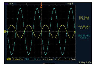
Fig. 5. Sine wave input (1 V peak-to-peak) and output (7 V peak-to-peak) waveforms recorded during the 430th hour of amplifier stage electric al operation at 500 °C.

Figs. 4, 5, and 6 briefly summarize the results of the simple voltage amplifier stage board constructed using a second 6H-SiC MESFET (Device #2). The amplifier board was subjected to 656 hours of unbiased 500 °C heat soaking prior to initiation of 500 °C continuous electrical operation. Fig. 4 shows the circuit schematic with the dotted box showing the parts of the circuit on the board tested in the 500 °C oven. For this initial low-frequency demonstration, the amplifier output wire was connected via RG-58 BNC cable directly into a 1 M-ohm AC-coupled digitizing oscilloscope input, and an external (room temperature) coupling capacitor was also required at the amplifier input as the 500 °C on-board capacitor was too small to support low-frequency (~100 Hz) operation [4]. Fig. 5 shows the sine wave input and output voltage waveforms measured in the 430th hour of continuous 500 °C electrical operation (in addition to 656 hours of unbiased 500 °C heat soak). Circuit power supply biases were held constant throughout the 500 °C electrical test duration. Fig. 6 shows measured voltage gain vs. frequency performance after various periods of continuous electrical operation at 500 °C. The amplifier gain remained stable (within 20% of original value) for over 600 hours of continuous 500 °C electrical operation (over 1300 hours total soak time at 500 °C). Between 668 and 1300 hours of electrically biased test time, a severe degradation in amplifier gain is observed. Curve-tracer characterization of MESFET Device #2 recorded at the beginning and end the 500 °C testing exhibited gate-leakageinduced I-V degradation qualitatively similar to the degradation illustrated in Fig. 2 for Device #1.

Fig. 6. Amplifer stage voltage gain vs. frequency for selected 500 °C electrical operating times up to 1300 hours. The amplifer was subjected to 656 hours of unbiased 500 °C heat soak prior to the electrical test.

Discussion and Summary

The primary mechanism limiting the duration of stable 500 °C electrical operation of the 6H-SiC MESFET was the increased current leakage from the transistor’s Schottky gate-to-channel junction. The increased gate leakage observed with 500 °C anneal time is generally consistent with previously observed behavior wherein this same metal-semiconductor interface gradually changed from Schottky to ohmic behavior with thermal annealing time [2]. Such gate leakage degradation should be greatly reduced via the fabrication of Junction Field Effect Transistors (JFET’s) that use SiC pn junctions as gates instead of metal-semiconductor junction gates. Therefore, fabrication of similar 6H-SiC JFET’s has been initiated with the goal of achieving even longer 500 °C operation. In summary, SiC MESFET electronics and packaging have demonstrated stable continuous electrical operation in a 500 °C oxidizing air ambient for over 2400 hours. Such electronic durability is sufficient for application to hot-section sensor signal conditioning electronics beneficial to turbine engine ground-testing.

Acknowledgements

This work was funded and carried out by NASA Glenn Research Center under the Glennan Microsystems Initiative, Ultra Efficient Engine Technology, Propulsion 21, and NASA Electronic Parts and Packaging programs. The authors greatly appreciate the contributions of E. Benavage, D. Lukco, A. Trunek, D. Androjna, C. Chang, M. Mrdenovich, B. Osborn, G. Hunter, and L. Matus.
Fuente: http://www.grc.nasa.gov/WWW/SiC/publications/ECSCRM06FET.pdf
Ver blogger original: http://nubia-anc.blogspot.com/

Multifunctional CuO nanowire devices: p-type field effect transistors


Doping is the most common way to produce p-type materials, but it can present many obstacles such as poor stability. An alternative approach is to exploit the p-type behaviour of CuO nanowires.

Nano lab team

Researchers at Nanyang Technological University, Singapore, grow high-quality CuO nanowires with high yield by heating copper foil in air. With the help of the standard UV lithography process, field effect transistors (FETs) based on individual CuO nanowires can be created.

Systematic investigations into electrical transport within the structures reveal that, without any further treatment, the as-grown CuO nanowires can perform as the channel material in p-type FET devices with mobilities of more than 2–5 cm2 V–1 s–1. The result highlights the potential of CuO nanowries to complement n-type semiconductor metal oxide nanowires in future integrated nanoelectronics.

The researchers can transfer their CuO nanowires to a standard silicon wafer with good alignment. In this way, thin-film transistors, which exhibit better performance than that of the single CuO nanowire FETs, can be readily fabricated. This study could pave the way for a large-scale manufacturing process for making high-performance p-type nanowire-based thin-film devices.

Another application that demonstrates the potential of such CuO nanowires is gas sensing. The researchers found that due to the selective adsorption of CO molecules on the surface of the nanowire, CuO could be used as a material for detecting carbon monoxide.

The group is focusing its efforts on exploring physical and biological properties of novel metal-oxide nanostructures and developing practical nanodevices.

About the author
The work was performed at the Physics and Applied Physics Division, School of Physical and Mathematical Sciences, Nanyang Technological University, Singapore. Dr Lie Liao is a Singapore Millennium Foundation Research Fellow working on the metal oxide nanostructures. Bin Yan is a PhD student with an interest in probing optical and electrical properties of metal-oxide nanostructures. Dr Ting Yu, the group leader, focuses on the metal-oxide nanodevices and graphene, in particular engineering band structures of graphene and developing graphene-based materials for new energy.

Ver blogger original: http://nubia-anc.blogspot.com/

Nanowire transistors outperform MOSFETs

Researchers at Harvard University, US, say they have made the best nanowire transistors to date. The devices consisted of germanium/silicon core/shell nanowire field-effect transistors (FETs) using high-κ dielectrics and a metal top gate geometry.

"We showed that our current Ge/Si nanowire FETs perform three to four times better than silicon CMOS [devices],"  Charles Lieber of Harvard told nanotechweb.org, "thus demonstrating for the first time that there is a clear advantage to nanowire versus conventional planar FETs.
This justifies further (aggressive) work on the nanowire FETs and, by reporting results in an industry standard, we hope we will also make industry better aware of the potential of this basic research." Lieber and colleagues used band structure design to create a hole gas in the Ge/Si core-shell system. "This has proved to be an ideal system with reliable ohmic contact and high mobility," said Lieber.

The researchers employed a benchmark typically used by the semiconductor industry to characterize the on-current and intrinsic delay properties of their devices. The transistors exhibited a scaled transconductance of 3.3 mS µm-1 and on-current of 2.1 mA µm-1. Hole mobility, meanwhile, was 730 cm2 V-1 s-1 – 10 times higher than that of a silicon p-metal-oxide semiconductor field effect transistor (MOSFET).

What's more, according to the scientists, the device's intrinsic switching delay was comparable to that of similar length carbon nanotube field-effect transistors and much better than the length-dependent scaling of planar silicon MOSFETs.
Lieber reckons the devices could have applications in next-generation high-speed logic circuits after conventional CMOS technology hits its limits. "In addition, the high-performance nanowire transistors can also [work] on many unconventional substrates, such as glass or plastic for transparent or flexible applications, where conventional crystalline Si technology is not possible," he added. "The excellent mobility exhibited by the nanowires would greatly improve device speed for these applications."

Now the researchers plan to improve the performance of the Ge/Si nanowire devices and scale them to smaller sizes; develop their ideas for other systems, for example by creating devices with a carrier gas of electrons rather than holes; and to create large-scale assemblies of the nanowire devices for integrated systems.

The researchers reported their work in Nature.

About the author
Liz Kalaugher is editor of nanotechweb.org.

Ver blogger original: http://nubia-anc.blogspot.com/

Carbon Nanotube Field Effect Transistor (CNT FET)

NNI Scientific Accomplishments 2009

Technology to Support National Security Space System Applications
Supporting/Contributing Agencies: National Reconnaissance Office

A critical need exists to improve satellite receiver front end performance for a variety of applications that include communications, imaging and signal acquisition. One of the most limiting features associated with operation of receiver systems is the non-linear behavior of components that process signals. Indeed, this non-linear behavior results in the generation of spurious signals that interfere with the detection of small, but critical signals and greatly limits performance, often identified as Spurious Free Dynamic Range (SFDR) with units of decibels.

CNT FET technology R&D has shown that these devices can provide almost linear operation over a wide range of input signal strengths, at low power operation, and thus, significantly improve the SFDR associated with receiver performance. These front end improvements can be directly translated to overall improvements in satellite system performance such as the detection of lower power signals, smaller satellite antenna size, lower system operating power requirements and the ability to discern very low strength signals in cluttered signal environments.

At present, efforts to develop and demonstrate CNT FET based very low noise linear amplifiers and signal mixers (circuits that combine two frequencies to produce a third frequency that is more amenable to signal processing) are in progress at Northrop Grumman Electronics Systems. Moreover, initial analysis indicates that a CNT FET mixer can provide as much a 40db improvement (a factor of 10,000) in SFDR, when compared to standard silicon based or gallium arsenide (GaAs) technology used for these types of applications. This would provide dramatic improvement in overall system performance. Additionally, it is envisioned that this same CNT FET technology can be used to fabricate devices that translate analog to digital signals (analog to digital converters) to support onboard processing with similar benefits. As a further benefit CNT FET technology should also be radiation resistant and thus, enhance satellite survivability.

Figure 1 – CNT FET Operation versus GaAs Comparing Operating Range as a Function Power

References/Publications
H. Zhang, et. al., “Low-Power High-Speed Carbon Nanotube Field Effect Transistors for

Fabricación de transistores de efecto campo con nanopuntos

Por Pedro Feijoó

En un artículo publicado por Japanese Journal of Applied Physics, Yijan Chen propone un método de fabricación de transistores de efecto campo mediante nanopuntos. Lo novedoso de este artículo es que tiene en cuenta la aleatoriedad del tamaño y de la posición de estas nanoestructuras en su proceso de fabricación.

En la figura está representado un transistor de efecto campo basado en nanopuntos. En él, dos capas de material (fuente y drenador) están conectadas mediante numerosos nanopuntos de material semiconductor. Los nanopuntos sólo conducen la electricidad cuando el material que los rodea (la puerta) está a un potencial que cumple una determinada condición. En la figura se puede observar que los nanopuntos más pequeños no llegan a conectar la fuente y el drenador. Sin embargo, se supone que en cada transistor hay tantos nanopuntos como para asegurar estadísticamente una conexión suficiente.

El material propuesto para realizar el transistor es silicio. Para un transistor tipo n, la fuente y el drenador son capas de silicio muy dopado tipo n y los nanopuntos, silicio dopado tipo p, que cumplen la función de canal. La puerta, que rodea a los nanopuntos, puede ser un metal o poli-silicio muy dopado. La puerta debe estar separada por un dieléctrico del canal, de la fuente y del drenador. En este caso, el dieléctrico más adecuado es el óxido de silicio.

Para fabricar el dispositivo deben darse una serie de pasos detallados en el artículo. En un principio, hay que crecer nanopuntos de silicio sobre una superficie de silicio muy dopado mediante algún método efectivo y fiable. Se pueden usar métodos como el auto ensamblaje o la implantación por haz de iones. Esta parte del proceso es la que más hay que desarrollar. Tras ello, hay que utilizar métodos típicos de la fabricación de los dispositivos de la nanoelectrónica actual que se han desarrollado en las últimas décadas, como son la deposición química de vapor (CVD), el pulido mecánico químico (CMP) y el ataque químico (etching).

Para el cálculo de parámetros importantes del transistor, como el área activa, se supone que el área total del transistor encierra un número muy grande de nanopuntos, cuyos tamaños siguen una determinada distribución de probabilidad. Por tanto, se pueden hallar valores esperables de las características del transistor a través de esta distribución de probabilidad determinada experimentalmente y que dependerá del proceso de fabricación de estas nanoestructuras.

Por otro lado, el autor del artículo desarrolla un modelo de la física del dispositivo. Resuelve la ecuación de Poisson en el interior de los nanopuntos consiguiendo una solución general analítica. La condición de contorno necesaria es que el potencial en el radio exterior del nanopunto es el potencial de la puerta.

Fuente:http://blogs.creamoselfuturo.com/nano-tecnologia/2008/04/25/fabricacion-de-transistores-de-efecto-campo-con-nanopuntos/
Ver blogger original: http://nubia-anc.blogspot.com/